Nanopatterning applications
SCIL Nanoimprint’s technological possibilities
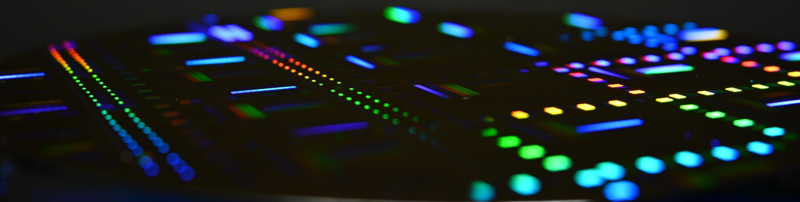
Building patterns and structures at the nanoscale allows to control and manipulate the light travel on materials to perform different kinds of devices in fields such as optics, electronics, biotechnology, and energy. Thus makes nanopatterning a key process step for a multitude of nanophotonic applications. The applications mentioned above are just some examples of SCIL Nanoimprint’s technological possibilities.

Optical I/O
Due to exponential growth of AI datacenters are faced with limits to the capacity of traditional copper communications infrastructure. Optical I/O has the potential to overcome these bottlenecks with higher bandwidth, low latency and energy efficient communications all the way down to the chip level.

Augmented Reality
Nowadays, creating interactive experiences in the real world is attracting more attention nowadays. Employing SCIL, AR devices can be manufactured highly reproducible without plastic deformation.

Metalenses
The conformal imprinting, high-resolution patterning, and the possibility of using complex patterns in addition to a wide range of materials make SCIL technology optimal for building metalenses.

VCSEL & PCSEL Lasers
The possibility of manufacturing gratings with sub-wavelength pitch avoids diffraction losses in the laser cavity, increasing its efficiency.

Bioapplications
Bioapplications play an important role in the human life and society. SCIL technology can be employed in biotech due to the possibility of using biocompatible materials and high-resolution nanopatterns.
Hence, it is possible to utilize it in the production of various devices such as sensors among other devices.

LED
The solid-state lighting revolution has been made possible with white LEDs. Using SCIL and metallic nanoparticles in a nanopattern, it is possible to increase the quantum emission intensity by up to 70 times to create more effective white LED sources.

Photonic crystals
SCIL technology for imprinting the nanopatterns makes possible to create periodic structures that allow controlling and manipulating the light wavelength and direction, thus modifying its propagation. Photonic crystals are interesting for lenses, mirrors or even paints and inks.
If you believe that the SCIL Nanoimprint’s technological possibilities are in line with your requirements, please don’t hesitate to contact us to discover how our technology can meet your specific needs!