Our facilities
Our facilities
SCIL Nanoimprint solutions provides its customers with everything they need – consumables, tooling & support- to achieve high-resolution nano-patterns on different substrates. A dedicated team that facilitates the production of your nanoimprints and takes them to the next level.

Efficient
Maximizing efforts to deliver
high quality products

Committed
Full dedication to helping our customers achieve optimal results

Skilled
Multidisciplinary talented team delivering solutions
SCIL’s extensive process knowledge in both pre and post-processing is a result of decades of experience in the field of nano-processing. Consequently, this knowledge provides benefits and advantages to our customers from the early proof of concept phase to the final goal of high-volume manufacturing.
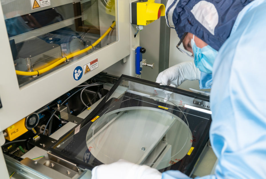
The SCIL application center, operating from The High Tech Campus in Eindhoven (The Netherlands), is equipped with everything you need to make collaboration with customers a great success. Moreover, in our application center, we have a multitude of analytical tools including (but not limited to) a high-resolution SEM and a state-of-the-art metrology tool by our partners from TeraNova. Therefore, you will have everything you need to characterize your high-resolution nano-patterns.
Pilot production
After completing the proof of concept phase, SCIL Nanoimprint solutions offers customers the possibility of pilot production at our facilities in Eindhoven. Using our patented resist and stamp combination up to 500 imprints can be done with just a single stamp without compromising structure fidelity. In addition, resists with a wide range of refractive indices, i.e. 1.25 – 2.0 in the visible spectrum, are available at SCIL for meeting the needs of a variety of customer applications.

x imprint wafers

< 1 µm
Alignment accuracy

100 to 300 mm
Wafer size