
Small world, performing big solutions
SCIL Nanoimprint solutions benefits
We combine the resolution and accuracy of rigid stamps with the flexibility of soft stamp methods. SCIL takes away all the drawbacks of rigid lithography, achieving nanometer resolution without the pattern deformation that other soft stamp methods suffer from.
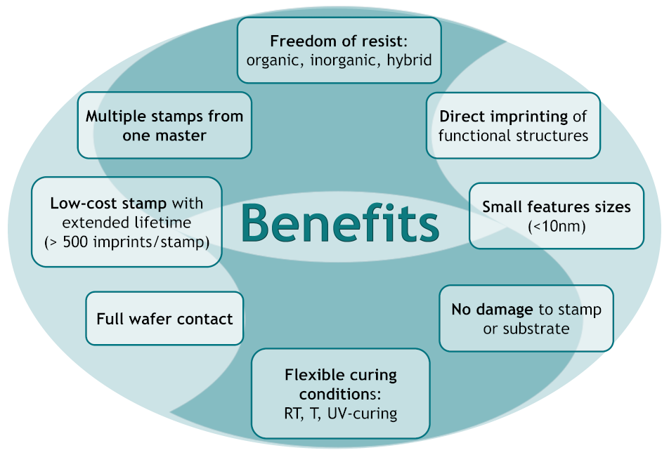
Our technology enables the direct stamping of nano- and micrometer-scale structures such as slanted, holes, 3D structures, lines/spaces and pillars: among other features. SCIL provides high-quality prints with full wafer contact in areas up to 300 mm, making patterns with feature sizes below 10 nm and an overlap accuracy of less than 1um on two sides of the wafer.
The use of a soft stamp and not high pressures means that no damage to the stamp or the substrate occurs. Moreover, the stamp has a high lifetime (>500 imprints/stamp), resulting in a low cost method. In addition, it is possible to make multiple stamps from the same master.
The composition of the imprint resist is not a problem since organic, inorganic, or hybrid resists can be used. Our technology, is compatible with other resists and different curing conditions (UV, T, RT curing).
Discover the full range of products SCIL Nanoimprint solutions has to offer to obtain high quality nanoimprints.